- 您现在的位置:买卖IC网 > Sheet目录114587 > 571MDAFREQDG (SILICON LABORATORIES) VCXO, CLOCK, 10 MHz - 945 MHz, LVPECL OUTPUT
Si570/Si571
24
Rev. 0.31
10. 8-Pin PCB Land Pattern
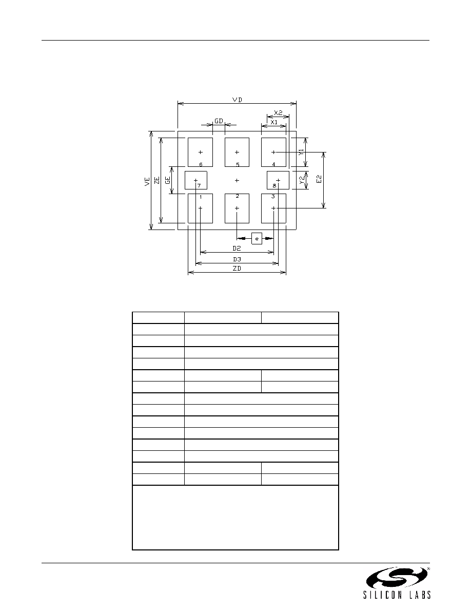
Figure 7 illustrates the 8-pin PCB land pattern for the Si570/Si571. Table 17 lists the values for the dimensions
shown in the illustration.
Figure 7. Si570/Si571 PCB Land Pattern
Table 17. PCB Land Pattern Dimensions (mm)
Dimension
Min
Max
D2
5.08 REF
D3
5.705 REF
e
2.54 BSC
E2
4.20 REF
GD
0.84
—
GE
2.00
—
VD
8.20 REF
VE
7.30 REF
X1
1.70 TYP
X2
1.545 TYP
Y1
2.15 REF
Y2
1.3 REF
ZD
—
6.78
ZE
—
6.30
Note:
1. Dimensioning and tolerancing per the ANSI Y14.5M-1994
specification.
2. Land pattern design follows IPC-7351 guidelines.
3. All dimensions shown are at maximum material condition
(MMC).
4. Controlling dimension is in millimeters (mm).
发布紧急采购,3分钟左右您将得到回复。
相关PDF资料
550ME614M400DGR
VCXO, CLOCK, 614.4 MHz, LVPECL OUTPUT
550MH040M000DGR
VCXO, CLOCK, 40 MHz, LVPECL OUTPUT
550MH166M628DGR
VCXO, CLOCK, 166.628 MHz, LVPECL OUTPUT
550ND125M000DGR
VCXO, CLOCK, 125 MHz, LVDS OUTPUT
550CJ153M600DGR
VCXO, CLOCK, 153.6 MHz, CMOS OUTPUT
550EJ100M000DG
VCXO, CLOCK, 100 MHz, LVPECL OUTPUT
550EK100M000DGR
VCXO, CLOCK, 100 MHz, LVPECL OUTPUT
550GD050M000DGR
VCXO, CLOCK, 50 MHz, CMOS OUTPUT
相关代理商/技术参数
571MDB000105DG
功能描述:VCXO振荡器 Prgramble VCXO 8pin 7mmx5mm RoHS:否 制造商:Fox 封装 / 箱体:5 mm x 3.2 mm 频率:19.2 Mhz 频率稳定性:2.5 PPM 输出格式: 封装:Reel 电源电压:3 V 端接类型:SMD/SMT 尺寸:3.2 mm W x 5 mm L x 1.5 mm H 最小工作温度:- 20 C 最大工作温度:+ 75 C
571MDB000105DGR
制造商:Silicon Laboratories Inc 功能描述:CNTRLD OSC 622.08MHZ VCXO LVPECL 8SMD - Tape and Reel
571MEA000107DG
制造商:Silicon Laboratories Inc 功能描述:OSCILLATOR - Trays
571MEA000122DG
制造商:Silicon Laboratories Inc 功能描述:CONTROLLED OSCILLATOR 1GHZ VCXO LVPECL 6-PIN SMD - Trays
571MEB000105DG
功能描述:VCXO振荡器 Prgramble VCXO 8pin 7mmx5mm RoHS:否 制造商:Fox 封装 / 箱体:5 mm x 3.2 mm 频率:19.2 Mhz 频率稳定性:2.5 PPM 输出格式: 封装:Reel 电源电压:3 V 端接类型:SMD/SMT 尺寸:3.2 mm W x 5 mm L x 1.5 mm H 最小工作温度:- 20 C 最大工作温度:+ 75 C
571MEB000105DGR
制造商:Silicon Laboratories Inc 功能描述:CNTRLD OSC 622.08MHZ VCXO LVPECL 8SMD - Tape and Reel
571MEB000852DG
制造商:Silicon Laboratories Inc 功能描述:OSCILLATOR - Trays
571MFB000325DG
功能描述:VCXO振荡器 PRGRMBL VCXO 8pin 7mm x 5mm RoHS:否 制造商:Fox 封装 / 箱体:5 mm x 3.2 mm 频率:19.2 Mhz 频率稳定性:2.5 PPM 输出格式: 封装:Reel 电源电压:3 V 端接类型:SMD/SMT 尺寸:3.2 mm W x 5 mm L x 1.5 mm H 最小工作温度:- 20 C 最大工作温度:+ 75 C